Deposition of metal, dielectric, and semiconductor thin films on substrates ranging from small chips to full 150 mm wafers.
Chemical vapor deposition (CVD)
Chemical Vapor Deposition (CVD) is a process used to produce high-quality, high-performance solid thin films and coatings. In CVD, gaseous precursors react or decompose on a heated substrate surface to form a solid material, while volatile by-products are removed by gas flow. It enables excellent conformity, uniformity, and material purity, making it ideal for semiconductor, MEMS, and nanotechnology applications.
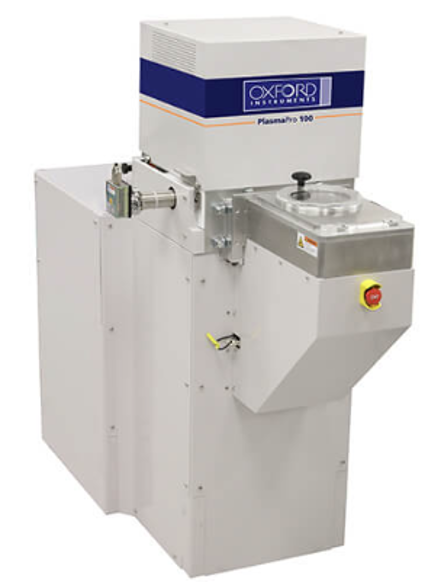
The Oxford PlasmaPro 100 Cobra 300 is primarily an Inductively Coupled Plasma (ICP) etching system, but it also supports plasma-enhanced chemical vapor deposition (PECVD) processes and allows low-temperature deposition of thin films such as silicon nitride (Si₃N₄), silicon dioxide (SiO₂), and amorphous silicon (a-Si:H). The high-density plasma ensures uniform coatings with excellent step coverage and adhesion, suitable for advanced microfabrication.
Electroplating
Electroplating is widely used for thin film deposition. In the ReynoldssTech electroplating bench, the target substrate is immersed in a chemical bath that contains dissolved metal atoms (such as copper, nickel, gold, aluminum, etc). An electric current applied between the target and the bath causes the atoms to deposit onto the substrate.
Get access – today!
Conconi Family BioDevice Foundry
SBME, UBC
![]() biodevice.foundry@sbme.ubc.ca
biodevice.foundry@sbme.ubc.ca
Directory
Fabrication & Prototyping
Biofunctionalization
Characterization
Resources & Services